Component Codesign Basics#
When we have photonic components driven by electronic devices, there is a scope that we might want to optimize certain devices to be faster, smaller, or less power-consumptive. It can be complicated to do this just analytically, so we would like to have the capability of integrating our design software for each of our devices with the simulation software of our electronics. There might be multiple software tools to design different devices, and the benefit of integrating these tools via open-source is that co-design becomes much more feasible and meaningful. I have explicitly made this example thorough for electronics engineers transitioning into photonic components engineering.
In this example, we will be exploring the co-design of a thermo-optic phase shifter in continuation of all the previous examples.
This example consists of a few things:
Connect a
gdsfactorycomponent to afemwellmodel, and relate the corresponding metrics.Extract a
hdl21 SPICEmodel from the generated component we can use in circuit simulators.Simulate the mode profiles via
Tidy3D FDTDand extract theS-Parametersfrom the layout.Create a flow where variations on both electronic and photonic parameters can be quantified through this model.
Good examples of sections of this flow are:
Some of the previous examples in
piel
There are some great resources to understand FDTD in the Tidy3D website. In particular, in relation to the flow you might use in piel, you might want to review:
Lecture 4: Prelude to Integrated Photonics Simulation: Mode Injection
The Finite-Difference Frequency-Domain Method, Hans-Dieter Lan
[ ]:
import gdsfactory as gf
[ ]:
# import gplugins.tidy3d as gt
import tidy3d as td
Getting Started with Mode Analysis#
In this section, we will demonstrate multiple aspects of a full design flow between photonic design tools, coupled to electronic design tools, starting from the basic first principles. In this case, we are extending gplugins alongisde the piel electronic modelling tools.
We want to understand the coupled analysis of the photonic performance of our components with variatations of their electrical design. There are multiple ways to perform mode analysis which TODO LINK FUNDAMENTALS PAGE. We will explore a fundamental one, which is 3D FDTD analysis. Fundamentally, it is a time-to-frequency pulse Maxwell’s equations accurate solver for 3D structures. We will use the Tidy3D plugin for this.
We can also compare this to other faster but less a bit less accurate mode solver techniques as described by the `femwell example <https://helgegehring.github.io/femwell/photonics/examples/waveguide_modes.html>`__.
We will begin by starting from the gplugins-Tidy3D structure.
Examining our Layer Stack#
We will use the gdsfactory layer default PDK layer stack. You might want to examine it because it has the thicknesses and positions of our layer. You can read more about it in the ``gdsfactory` documentation <https://gdsfactory.github.io/gdsfactory/notebooks/03_layer_stack.html>`__.
[ ]:
gf.config.rich_output()
# PDK = gf.generic_tech.get_generic_pdk()
# PDK.activate()
# LAYER_STACK = PDK.layer_stack
# LAYER_STACK
We will also set the resolution of our mesh for the components we care about for the femwell PDE solver:
[ ]:
resolutions = {
    "core": {"resolution": 0.02, "distance": 2},
    "clad": {"resolution": 0.2, "distance": 1},
    "box": {"resolution": 0.2, "distance": 1},
    "slab90": {"resolution": 0.05, "distance": 1},
}
Starting where we always do: our heated MZI2x2#
We want to model our heated MZI2x2 phase shifter.
[ ]:
our_heated_mzi2x2 = gf.components.mzi2x2_2x2_phase_shifter()
our_heated_mzi2x2.plot()

[ ]:
from gdsfactory.export import to_svg
[ ]:
to_svg(
    our_heated_mzi2x2,
    filename="../_static/img/examples/03a_sax_active_cosimulation/mzi2x2_phase_shifter.svg",
)
However, we know from the instances list that the heater element in our MZI2x2 is a straight_heater_simple
[ ]:
our_heated_mzi2x2.settings.full
{
    'delta_length': 10.0,
    'length_y': 2.0,
    'length_x': 200,
    'bend': {'function': 'bend_euler'},
    'straight': {'function': 'straight'},
    'straight_y': None,
    'straight_x_top': 'straight_heater_metal_simple',
    'straight_x_bot': None,
    'splitter': {'function': 'mmi2x2'},
    'combiner': {'function': 'mmi2x2'},
    'with_splitter': True,
    'port_e1_splitter': 'o3',
    'port_e0_splitter': 'o4',
    'port_e1_combiner': 'o3',
    'port_e0_combiner': 'o4',
    'nbends': 2,
    'cross_section': 'strip',
    'cross_section_x_top': None,
    'cross_section_x_bot': None,
    'mirror_bot': False,
    'add_optical_ports_arms': False
}
[ ]:
our_heated_mzi2x2.settings.full["straight_x_top"]
So let’s see our heater component:
[ ]:
from piel import straight_heater_metal_simple
[ ]:
our_heater_component = straight_heater_metal_simple()
our_heater_component.plot_widget()
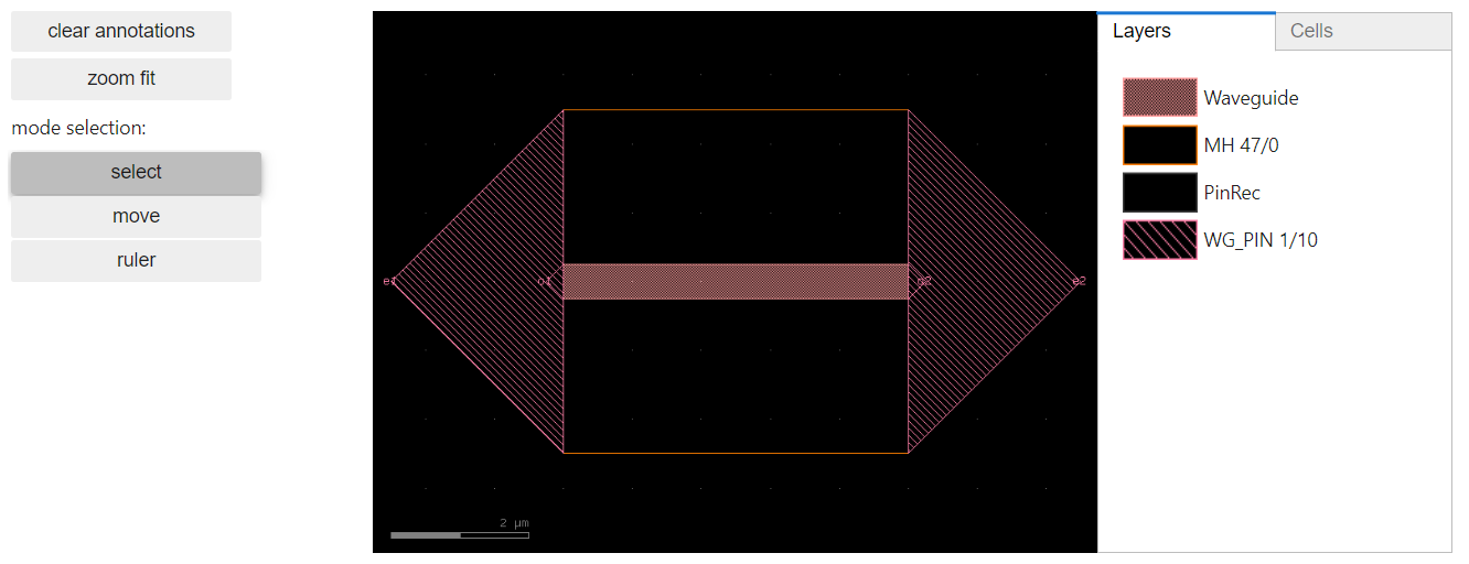
You can play around with the widget or Klayout view and notice that this phase shifter component is just a waveguide with a resistive metal trace on top.
Let’s get the properties of our waveguide and heater width.
[ ]:
our_heater_component.metadata
For example, we know these are the layers in our heater.
[ ]:
our_heater_component.get_layer_names()
['MTOP', 'VIA1', 'M2', 'HEATER', 'VIA2', 'WG_PIN', 'WG']
These are the layers we need to account for.
However, there is more. The waveguide path, if you look closely on the geometry, is extruded from what we call a gf.CrossSection which is basically just a description of a layer path geometry for a particular trace. This cross sectional view is what we use to simulate infinitessimal sections of our devices for multiple physics. We create metrics per length, and it is reasonable to extend these infinitessimal metrics for a particular total path length whenever the cross section is invariant.
In our example, the cross-section we care about is called the strip_heater_metal:
[ ]:
our_heated_waveguide_cross_section = gf.get_cross_section(
    our_heater_component.metadata["default"]["cross_section_waveguide_heater"]
)
our_heated_waveguide_cross_section
You can also access this from it’s function call:
[ ]:
gf.cross_section.strip_heater_metal(
    heater_width=2.5,
)
Let’s make a basic straight waveguide using this cross section for reference:
[ ]:
our_heated_waveguide_straight = gf.components.straight(
    length=5,
    cross_section=gf.get_cross_section(
        our_heater_component.metadata["default"]["cross_section_waveguide_heater"]
    ),
)
our_heated_waveguide_straight.plot_widget()
This small cross-sectional view matches much more easily with the infinitessimal component simulation tools.
Getting Started with FDTD in this flow#
Our heater is implemented on a standard SOI waveguide that has a silicon core with a silica cladding, and the material files is the same as from the gt.materials.get_index("SiO2") in gplugins Tidy3D functionality. However, this time we will use the cross sectional view specific to our heater implementation including the metal on the top as we want a complete simulation that considers the electrical performance. `
Let’s assume our heater is not made from TiN as in the default PDK, but we want to create it from one of the materials in the Tidy3D material library:
[ ]:
td.material_library.keys()
So let’s change our layer stack from our gdsfactory.generic_pdk to simulate this. We can also change the position of the metal in relation to the waveguide. This, for example, would tell us the effect of optical loss from evanescent field absorption for different materials, and would allow us to extract component properties we can use in sax for photonic network analysis accordingly. Let’s make a function of heater parameters we can use to create a Tidy3D simulation from it’s
parameterised outputs:
[ ]:
def change_heater_properties(
    heater_material_name: str,
    heater_material: gt.materials.MaterialSpecTidy3d,
    heater_width_um: float = 2.5,
    heater_zmin_um: float = 0.5,
    heater_thickness_um: float = 0.13,
    layer_stack=None,
) -> tuple:
    """
    This function perturbs the provided layer stack and changes specific heater layer parameters.
    We will also return a cross section of the heater width.
    """
    if layer_stack is None:
        layer_stack = gf.generic_tech.get_generic_pdk().layer_stack

    material_name_to_tidy3d = {
        "Aluminum": td.material_library["Al"]["Rakic1995"],
        "si": td.material_library["cSi"]["Li1993_293K"],
        "sio2": td.material_library["SiO2"]["Horiba"],
        "sin": td.material_library["Si3N4"]["Luke2015PMLStable"],
        # "TiOx": td.material_library["TiOx"]["HorbiaStable"],
        heater_material_name: heater_material,
    }

    # Change default heater cross section properties

    cross_section = gf.cross_section.strip_heater_metal(
        heater_width=heater_width_um,
    )

    # Change heater layer stack and material properties in PDK definition
    layer_stack.layers["heater"].material = heater_material_name
    layer_stack.layers["heater"].thickness = heater_thickness_um
    layer_stack.layers["heater"].zmin = heater_zmin_um

    heater_waveguide_straight = gf.components.straight(
        length=5, cross_section=cross_section
    )
    return (
        layer_stack,
        material_name_to_tidy3d,
        cross_section,
        heater_waveguide_straight,
    )
[ ]:
(
    LAYER_STACK,
    material_name_to_tidy3d,
    heater_cross_section,
    heater_waveguide_straight,
) = change_heater_properties(
    heater_material_name="TiOx",
    heater_material=td.material_library["TiOx"]["HorbiaStable"],
    heater_width_um=5,
    heater_zmin_um=2.5,
    heater_thickness_um=0.13,
)
You can explore the properties of the layer stack through some functions:
[ ]:
heater_waveguide_straight.plot_widget()
[ ]:
LAYER_STACK.get_layer_to_thickness()
[ ]:
LAYER_STACK.get_layer_to_material()
[ ]:
LAYER_STACK.get_layer_to_zmin()
[ ]:
LAYER_STACK.get_layer_to_sidewall_angle()
It is not a great idea to simulate our full heater component with vias and everything, as really there is no need if you understand the fundamental heater-cross section design. We can simulate only a small straight cross section of our waveguide.
[ ]:
our_heater_straight_cross_section_tidy3d_simulation = gt.get_simulation(
    heater_waveguide_straight,
    is_3d=True,
    material_name_to_tidy3d=material_name_to_tidy3d,
    plot_modes=True,
)
our_heater_straight_cross_section_tidy3d_simulation_plot_xz = gt.plot_simulation_xz(
    our_heater_straight_cross_section_tidy3d_simulation
)
our_heater_straight_cross_section_tidy3d_simulation_plot_yz = gt.plot_simulation_yz(
    our_heater_straight_cross_section_tidy3d_simulation
)
# Save our figures
our_heater_straight_cross_section_tidy3d_simulation_plot_xz.savefig(
    "../_static/img/examples/06_component_codesign_basics/our_heater_straight_cross_section_tidy3d_simulation_plot_xz.PNG"
)
our_heater_straight_cross_section_tidy3d_simulation_plot_yz.savefig(
    "../_static/img/examples/06_component_codesign_basics/our_heater_straight_cross_section_tidy3d_simulation_plot_yz.PNG"
)
Effective index of computed modes: [[2.4610755 1.8116093]] 
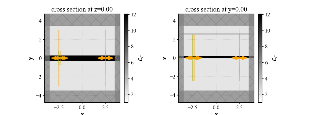
You can see the heater structure on the grey layer above the waveguide. Note that the calculated effective index of Mode 0 is near to the neff = 2.443 from Figure 3.14 of Silicon Photonics Design by Chrostowski. In the yz plane on the above image, we can see most of the light being confined in the core and cladding by the \(E_y\) field amplitude. On the higher order mode index 1, we can see that the top and bottom of the waveguide have a much more important effect of guiding the
mode in the \(E_z\) direction. We can also see the first-order mode profile on a smaller fraction of the light in the \(E_y\) mode.
Starting from our heater geometry#
We will create a function where we change the properties of the heater such as thickness and width, and we explore the change in resistance, but also in thermo-optic phase modulation efficiency, and the effect it has on the effective index and mode profiles through FDTD. So, we want to have some easy functions that allow us to easily mesh a component because we plan to do a few variations and connect the different simulation tools.
our_heater_mesh = our_heated_waveguide_straight.to_gmsh( type="uz", layer_stack=LAYER_STACK, xsection_bounds=[(4, -4), (4, 4)], ) our_heated_waveguide_straight.draw()TODO we should match the mesh between femwell and between Tidy3D for most accuracy in cosimulation.