Fundamental Co-Design Principles Theory#
It is important to understand the fundamental physical relationships of consigning photonics and electronics systems. Really, we are combining two engineering fields: photonics engineering and electronics engineering. The overlap between the fields, and interconnected relationships, are essential to optimise the system design between them.
A primer on common photonic-electronic systems#
We will explore some common photonic-electronic systems and discuss the design flows involved afterwards.
An Opto-Electronic System#
A relatively-common system is one where an electronic signal is generated from a photonic device. This involves the readout of photodetectors such as silicon photodiodes, photoresistors, or more-quantum-focused single-photon detectors such as superconducting nanowires. TODO ref.
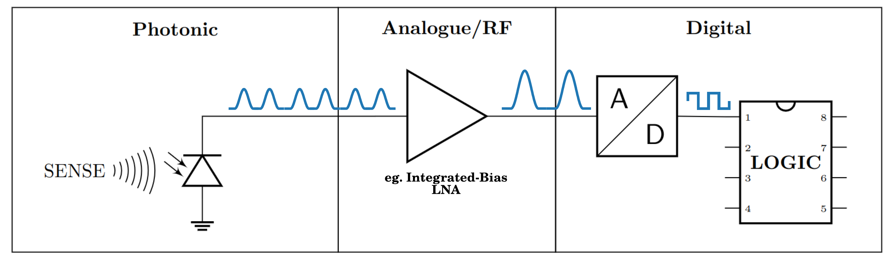
For many of these photodetectors, they need to be biased or amplified with analogue or RF electronics. This is often discretized into digital electronics through an equivalent ADC.
These systems are commonly used as sensing-based detectors, and can be used for very precise metrology. TODO add ref.
An Electro-Optic System#
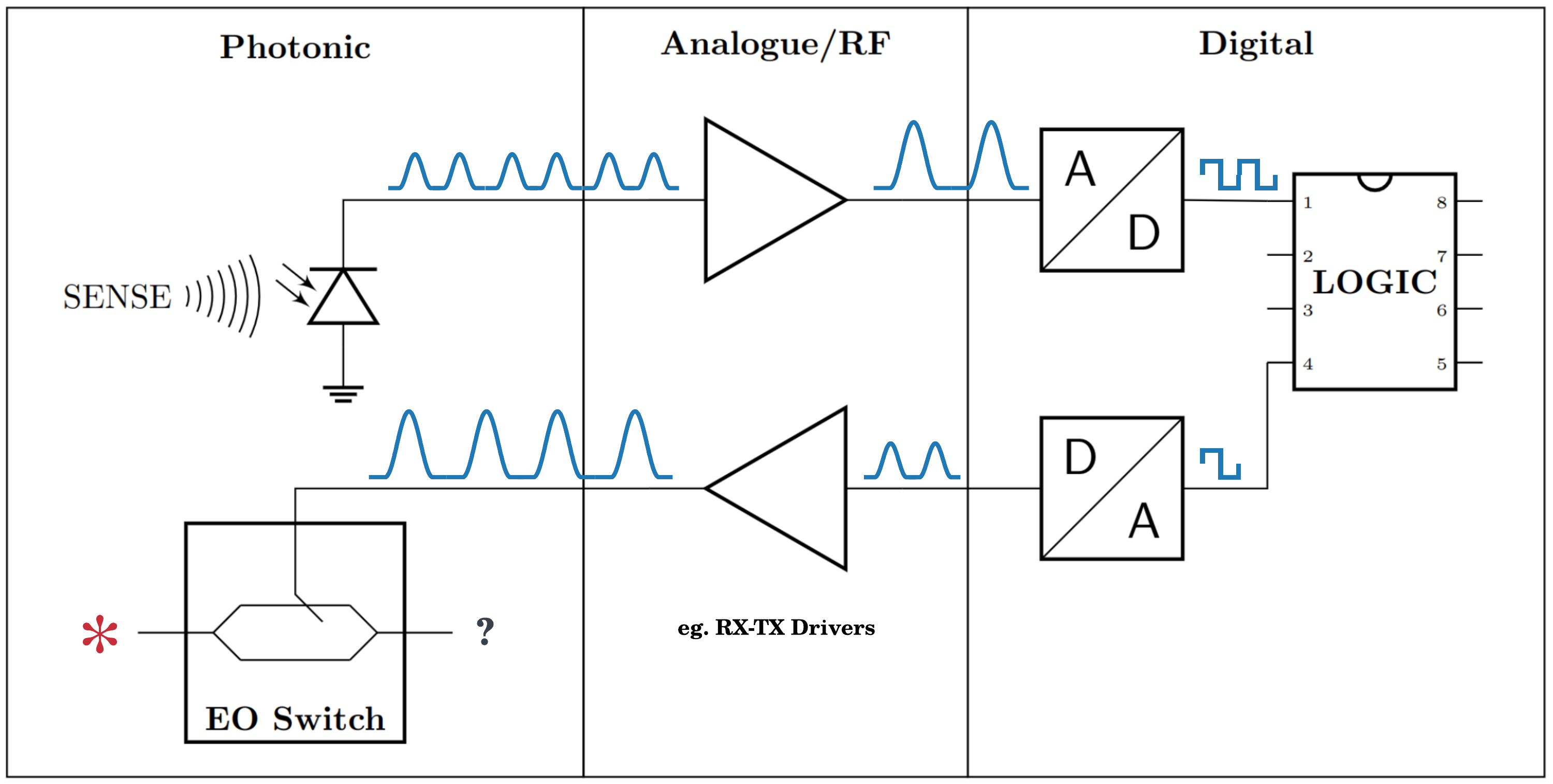
Another common system in the integrated photonics domain is an electronically-controlled photonic system. In this case, en electronic signal can control an optical signal such as a laser pulse, continuous laser, or more-quantum-focused single-photon and change it’s properties such as phase or amplitude.
These types of systems are more common in datacenters, photonics-driven-HPC, neuro-morphic photonic computation, and quantum photonic systems. TODO ref.

To optimise power consumption, it might be desired to design custom digital logic, with custom amplifiers and specifications, for a application-specific integrated photonic device.
In an integrated-photonics platform, it is common to use a Mach-Zehnder interferometer as en electro-optic switch. This is by the use of an active electro-optic or thermo-optic phase shifter on one interferometer arm, can be use to route a photonic path output or not.
A Concurrent Photonic-Electronic System#
These are the most interesting ones in my opinion. Concurrent photonic-electronic systems involve the interaction between optical signals and electronics signals in real-time, with feedback and feedforward. This is currently at the cusp of scientific development of current technology.
However, these systems are very hard to simulate fully. It involves the time-domain interaction of analogue, digital and photonic signals in order to model a specific behaviour. These are the type of systems we are interested in modelling through piel. The flexibility of open-source software enables us to create these type of modelling systems in a way that closed-source software can make it very difficult to extend.
Reference Applications#
What are some example applications of electronic-photonic codesign? Let’s look at some references and a brief summary of contents. Last updated: 06/2024.
Domain |
Reference |
Brief Description |
|---|---|---|
Communications |
Kim, Gyungock, et al. “Single-chip photonic transceiver based on bulk-silicon, as a chip-level photonic I/O platform for optical interconnects.” Scientific Reports 5.1 (2015): 11329. |
|
Communications* |
Sengupta, Kaushik, Tadao Nagatsuma, and Daniel M. Mittleman. “Terahertz integrated electronic and hybrid electronic–photonic systems.” Nature Electronics 1.12 (2018): 622-635. |
|
Foundry |
KIMERLING, L. C., et al. Electronic-photonic integrated circuits on the CMOS platform. En Silicon photonics. SPIE, 2006. p. 6-15. |
|
Foundry |
Orcutt, Jason Scott. Monolithic electronic-photonic integration in state-of-the-art CMOS processes. Diss. Massachusetts Institute of Technology, 2012. |
|
HPC |
YING, Zhoufeng, et al. Electronic-photonic arithmetic logic unit for high-speed computing. Nature communications, 2020, vol. 11, no 1, p. 2154. |
|
HPC |
Chen, Luis, et al. “Electronic and photonic integrated circuits for fast data center optical circuit switches.” IEEE Communications Magazine 51.9 (2013): 53-59. |
|
HPC & Neuromorphic AI |
Ning, Shupeng, et al. “Photonic-Electronic Integrated Circuits for High-Performance Computing and AI Accelerator.” arXiv preprint arXiv:2403.14806 (2024). |
|
HPC & Neuromorphic AI |
Xu, Bo, et al. “Recent progress of neuromorphic computing based on silicon photonics: Electronic–photonic Co-design, device, and architecture.” Photonics. Vol. 9. No. 10. MDPI, 2022. |
|
HPC & Neuromorphic AI |
Shastri, Bhavin J., et al. “Photonics for artificial intelligence and neuromorphic computing.” Nature Photonics 15.2 (2021): 102-114. |
|
Photonic Computation |
Macho‐Ortiz, Andrés, et al. “Analog Programmable‐Photonic Computation.” Laser & Photonics Reviews 17.10 (2023): 2200360. |
|
Photonic Computation |
Cheng, Junwei, Hailong Zhou, and Jianji Dong. “Photonic matrix computing: from fundamentals to applications.” nanomaterials 11.7 (2021): 1683. |
|
Signal Processing |
KÄRTNER, F. X., et al. Photonic analog-to-digital conversion with electronic-photonic integrated circuits. En Silicon Photonics III. SPIE, 2008. p. 59-73. |
Passive Photonics Design Applications#
Domain |
Reference |
Brief Description |
|---|---|---|
Design Flows#
Let’s consider the fundamental principles between electronic-photonic codesign flows, and the corresponding modelling at each stage. In this section, we will explore some design flow relationships between co-designed systems.
In pure mixed-signal microelectronics, there are already some established design flows normally for systems in the same chip.
For example: - Cadence Mixed-Signal Implementation Options - Cadence Verification Overview Whitepaper - Demystifying Mixed-Signal Simulation for Digital Verification Engineers
There is also some further work in the direction of silicon chiplet design, where different chips are connected together in an interposer to form a system rather than on a single-die. This is pretty handy for multi technology chips.
For example, - Building An Open Chiplet Economy - ZeroAsic Chiplet Solution
Eventually, in photonics, we will want to jump on this bandwagon, and there is some movement in this direction anyways.
So let’s summarise the existing mixed-signal design flows we know from these above:
Domain Principles#
There are three important domains in a given co-design flow: digital and analogue electronics, and photonics.
The photonics domain can be divided into passive photonics, not discussed here, and active photonics. Active photonics could be grouped into opto-electronic and electro-optic systems. Opto-electronic systems involve an optical signal being converted into a photonic signal, whilst electro-optics is the inverse.
Frequently, an analogue electronic signal drives or is generated by an active photonic device. For now, we will concern ourselves with analogue electronic signals that operate at multiple order of magnitude below of the frequencies of tera-hertz optical electromagnetic signals. However, there has been much research into the interaction of terahertz electronics and photonics which has led to interesting physical effects and applications, but maybe we discuss this in another section.
If we are interacting with these analogue signals through a modern computer, it means that we are discretising the analogue signals. In many applications, we need to consider the digital-logic control or readout of analogue signals from a photonic system.
Electronic Fundamentals#
Fundamental Electronic Definitions#
Read more in The Art of Electronics by Paul Horowitz and Winfield Hill.
There are some important definitions we must account for in terms of analysing the data of our simulations.
Term |
Definition |
Unit |
|---|---|---|
Voltage \(V\) |
The work on electric charges. |
It takes \(1J\) Joule to move \(1C\) Coulomb of charge through a potential of \(1V\) volt. |
Current \(i\) |
The rate of the flow of electric charge past a point. |
\(1A\) amp defines the movement of the above \(1C\) Coulomb of charge flows in \(1s\) second. |
Power \(W\) |
For a differential of time, this is the rate energy consumed for that slice of time. |
\(W = VI\) Watt defines the rate of energy flow of the above \(1J\) Joule in \(1s\) second. |
Energy \(J\) |
Applied power throughout a slice of time. |
\(J = Ws\) Joule is equal to \(1W\) Watt of power flowing throughout \(1s\) second. |
Currents occur by placing a voltage through a device, and the rate of the current, hence the rate of the power consumption is dependent on the channel impedance. Now, this has an important effect on microwave engineering and system design. Let’s consider some unit conversion, since it is important particularly between relating time and frequency, and DC and RF metrics.
Passives#
Read further in Digital Integrated Electronics by Jan Rabaey.
It is important to understand the relationship between electrical models of physical geometrical designs in relation to their photonic operation. Multiple photonic electronic-related layers have different resistive and inductive relationships. The interconnection mechanism has an effect on the propagation delay, power consumption, and noise.
Each wire has parasitic capacitance’s, resistances, and inductance. We need to account these differential circuit elements as points within the lab. Note that the wire parasitic capacitance is three-dimensional. Ideally, we can extract this information through RCX of the circuit.
Simple Capacitive Modelling#
TODO add figure
When electrical field lines are orthogonal, we can account for the width \(W\), length \(L\), dielectric constant \(\epsilon\) between the metal plates, and the thickness of the dielectric \(t\).
This is coupled to the resistivity \(\rho\) of the wire with the thickness of the metal \(H\) and width \(W\) to determine the its cross sectional area \(A\).
However, because we know the thickness for any particular metal \(H\), we can determine the resistance of a wire just from the geometry. Normally, these material parameters are determined in the form of a \(R_{\square}\) resistance.
Digital Design Metrics#
Read further in Digital Integrated Electronics by Jan Rabaey.
Say we have a digital switch gate. We apply a transition signal from low to high. The time in between 50% of the input signal and 50% of the output signal is called the propagation delay. However, rising (\(t_{pLH}\)) and falling (\(t_{pHL}\)) propagation delays tend to be different in physical components.
We define the propagation delay of the gate as the average of the two propagation delays:
TODO add figure.
The rise and fall times are a function of the strength of the driving gate, the load gate capacitance which is related to the fanout, and the resistance of the interconnect. In CMOS, there is a direct relationship between the gate drive strength and gate capacitance.
System Metrics#
Let us first begin considering the digital design metrics that are important for us to understand the electrical operation characteristics of mixed electronic-photonic systems. Most of these are redefined to include photonic loads based on Digital Integrated Circuits, A Design Perspective by Jan Rabaey. Page numbers are provided accordingly.
Power Consumption Definitions#
Peak Power#
A design can have a peak power \(P_{peak}\) which basically involves the maximum power consumption possible by the total photonic and electronic system. If we have a single supply voltage to our system \(V_{supply}\), then we can define it as:
If we have \(N\) multiple supply voltages to our system, which is more likekly the case in a mixed-signal digital and analogue supplies, and potentially another external photonic electrical supply, then we can define the total peak power of the system as:
In reality, we need to think of the maximum power that can be drawn by the maximum power consuming operation, which may not involve all supplies operating at the maximum draw. However, if you want a conservative estimate, you can assume that is it possible that all supplies are operating at their maximum current draw \(i_{peak}\). An generic maximum power defined as the highest consuming state of the system, where not all supplies are operating at their maximum \(i_{peak}\) power can then be defined dependent on an consumption efficiency parameter \(\eta_N\) for the highest operation load:
Average Power#
What may be more likely is that you might be operating this integrated electronic-photonic system with a set of instructions over a long period of time. A set of example of this would be through encoding communication channels, or arbitrary unitary operations, sensing a sample, etc. In this case, there is a power consumption over a period of time. We can describe this in terms of the average power consumption of the whole system over a period of time \(T\):
If we have multiple supplies, as is likely to be the case, then we can consider it to be:
Power Consumption Sources#
In terms of photonic loads#
We can decompose this in terms of dynamic and static power. When some transistors are switching, they are consuming dynamic power that they do not consume when they are in an idle state. This applies similarly to a photonic load. A resistive photonic load such as a thermo-optic heater is consuming power in an idle state constantantly whenever any signal is being applied. A capacitive load such as a electro-optic carrier depletion phase shifter gets charged and discharged according to the voltage that is applied and the total power consumption is dependent on the total switching events. The same could be said for the thermo-optic phase shifters in terms of a PWM-based modulation and so on. It is just important to understand the sources of power consumption and heat dissipation in our circuits in order for us to be able to optimise for it.
We know we want to minimise the static power consumption of the circuit on the idle state, which means that resistive loads such as heaters are no-gos in terms of VLSI-photonics without a suitable cooling solution.
In terms of dynamic loads, we know that the more switching events we have, and more components we have, the higher the total power consumption.
Let us evaluate how our circuit operates for these devices. In terms of a carrier depletion modulator, we can consider the electrical connection as some resistive wire and the junction load to be a capacitor. We can describe this from first-principles as a basic RC circuit, with the following relationship:
Our time constant \(\tau = RC\). And we know that \(50\% V_{out,RC} = 0.69\tau\) and \(90\% V_{out,RC} = 2.2\tau\) based on Eq. 1.13, page 34 on Rabaey.
Energy input from signal source to charge a capacitor, independent of series resistance R, although this determines rise times.
During charge-up, the energy stored in resistor is:
The other half of the energy gets dissipated in the resistor during rising edge, and the rest of the capacitor energy gets dissipated on the falling edge. This means that per transition there is about \(E_{load,loss} = \frac{CV^2}{2}\) of energy dissipation. This does not account the energy dissipation per stage, but we need to account for it for a super low power based design. There is also the characterisation considerations, and corresponding capacitances.
Another important relationship of the \(RC\) time constant is also in the driving of the device, when, in a switching event, the driving switch can be considered as a voltage-controlled-capacitor (gate) modulating-resistor (source-drain). This is important because we can see, when we drive a switching event, and when we consider our signal drivers, the effect of their fundamental components on the rest of the circuit.
Time Analysis#
Signal Propagation Definitions#
Our signals will change given that we have control over how we affect our photonic circuit. Say, we define two boundary conditions of our signals in a transition between 10% and 90%. We define the time of change in between these transitions as the rise or fall time depending on the direction of the change. In digital electronics, section 1.3 of Rabay, we call this change the propagation delay of our transitions. Now, this is very important for a range of reasons.
Mainly this has an effect on the speed of our system, and also on the power consumption of the system. It has an important effect on how we design our driving electronics for our photonics loads.
Rabay describes the importance of this definition very well:
The rise/fall time of a signal is largely determined by the strength of the driving gate, and the load presented by the node itself, which sums the contributions of the connecting gates (fan-out) and the wiring parasitics.
We will explore this definition in the context of our drivers and loads thoroughly. An important relationship worth remembering is that in a simple RC series circuit, it takes \(2.2 \tau = 2.2 RC\) to reach the 90% signal transition point.
This means that when digitizing the time of an RC signal in terms of defining the time step of our SPICE simulation, we need to decide the amount of resolution between the RC metric as a fraction of the RC time constant.
We go back to our basics by remembering some relationships in the The Art of Electronics by Paul Horowitz and Winfield Hill.
Low-Pass RC Filter#
TODO ADD IMAGE
In a low-pass series RC circuit filter common in P/EIC layout, the following transfer function relationships are also important. This is the equivalent circuit formed in between a signal routing wire, eg. DC wire to a heater, and the return path capacitive coupled signal. This relationship is also significant when deriving transmission line design parameters, but we will discuss this later.
This low-pass filter passes lower frequencies and blocks higher frequencies depending on the time constant of the circuit. Note that the capacitor has a decreasing reactance (the complex impedance component \(X_C\)) with an increasing frequency. Unless it is specifically designed for higher RF frequencies you must take care of what bandwidths you will operate your circuit. A common scenario of this would simply be the bandwidth of the wiring of the chip.
The transfer function of the output voltage node \(V_{out,RC}\) in between the \(RC\) elements in the frequency \(\omega\) domain:
RC Time-Constant Derivation#
The time constant relationship \(\tau\) is derived from this relationship. Note that at lower frequencies the capacitors reactance \(X_C\) is very high, which means that the output node is like a voltage divider with a small resistance on top of a very high one. However, at higher frequencies, this becomes less valid as \(X_C \approx \frac{1}{\omega C}\). This means that there will be a frequency \(\omega_0 = \frac{1}{RC}\)
High-Pass RC Filter#
TODO ADD IMAGE
In this case, the capacitor is connected directly to the input voltage \(V_{in}\) which provides an inverse relationship to the low-pass filter. The transfer function can be defined as:
Depending on your wiring, a common case of this type of filter might involve driving a capacitive load such as electro-optic modulator in the frequency domain. Note, it is possible to drive them in DC.
Driving, Propagation Delay & Fanout#
If we consider each of our modulators, as a load, we must also consider how we are driving them.
Device Physics#
Ideal 1D pn junction#
A pn junction is a building block for most electronic components, such as diodes and transistors.
Let’s discuss what doping is. We have some bulk silicon. In a perfect pure silicon crystal lattice, the six valence electrons of each silicon atom form covalent bonds with the valence electrons of its four nearest neighbors. This is the intrinsic state of silicon. The intrinsic electron carrier concentration of this semiconductor is defined by \(n_i\). However, when we dope silicon, normally at high temperatures with some other material, the lattice properties change and we change the number of free electrons in the lattice.
When we p dope some silicon, we tend to do this with materials that have one less valence electron than silicon, such as boron. This means that when we dope silicon with boron, we create a hole in the lattice.
When we n dope some silicon, we tend to do this with materials that have one more valence electron than silicon, such as phosphorus or arsenic. This means that when we n dope silicon, we create an extra electron in the lattice.
If we put a p doped silicon crystal next to an n doped silicon crystal, we create a pn junction. The electron concentration gradient is very large in between these regions. We describe the free electron concentration, the donor concentration, as \(N_D\). We describe the hole concentration, the acceptor concentration, as \(N_A\). Under zero voltage bias, the depletion region voltage defined by \(\phi_0\) is a function of the temperature, the intrinsic carrier concentration, and the donor and acceptor concentrations.
The thermal voltage is defined by \(\phi_T\) and is a function of the temperature \(T\), the charge of an electron \(q\), and the Boltzmann constant \(k\).
Depletion Region vs Voltage Bias#
Circuit Models#
Static MOS Transistor#
NMOS Switch Model#
TODO finish modelling equations
Photonic & RF Fundamentals#
Let’s review some theory on photonic and RF network design based on Chrostowski’s Silicon Photonic Design and Pozar’s Microwave Engineering. Optical and radio-frequency signals are both electromagnetic, within different orders of magnitude of frequency. The electro-magnetic theory principles are very similar, albeit there are different terminologies for some very similar things. We need to understand crucial differences between photonic and RF network design in order to properly design coupled electrical-photonic systems.
It is also important to understand electromagnetic propagation representation when we consider the simulation methodologies implemented by different solvers.
What is an electromagnetic wave?#
A Scottish man named James Clark Maxwell knew, and because of him so do we:
Note the units:
\(\mathcal{E}\) electric field in volts per meter \(V/m\)
\(\mathcal{H}\) magnetic field in amperes per meter \(A/m\)
\(\mathcal{D}\) electric flux density in Coulombs per meter squared \(C/m^2\)
\(\mathcal{B}\) magnetic flux density in Webers per meter \(Wb/m\)
\(\mathcal{J}\) electric current density in amperes per meter squared \(A/m^2\)
\(\mathcal{\rho}\) electric charge density in Couloms per meter cubed \(C/m^3\)
A sinusodial electric field polarised in the \(x\) direction can be generically written as:
where \(A(x,y,z)\) is the amplitude function dependent on spatial dimensions, \(\omega\) radian frequency, and \(\phi\) phase reference shift from the wave at time \(t=0\). The wave is polarised because only the \(\hat{x}\) component of the amplitude function is relevant.
Can we simplify this for our applications?#
For an isotropic, homogeneous medium where the signal wavelengths do not interact with nonlinear material properties, we can solve Maxwell’s curl equations in a phasor form known as the Helmholtz equations. This is not always valid for photonic network analysis as there can nonlinear material interactions such as spontaneous four-wave mixing and we will explore this afterwards, and is an approximation more common to radio-frequency analysis.
These equations can be thought of as simultaneous equations. With some vector calculus, they can be solved into:
The wavenumber constant \(k = \omega \sqrt{\mu\epsilon}\) relates the material dielectric constant \(\epsilon\) and magnetic permeability \(\mu\) to a travelling plane electromagnetic wave in any medium. This is also called the propagation constnat to describe how the wave changes with distance \(z\).
A general solution#
We can say that this definition is valid for every spatial component of the field.
Solving the above equation as a partial-differential-equation with separation of variables as done by Microwave Engineering by Pozar we can derive that the total wave propagation constant is directionally composed:
We can write the electric field component in the \(x\)-direction as a function of the electric field in space coordinates (\(x\), \(y\), \(z\)) due to the \(k(x,y,z)\)
Helmholtz’s on a lossless waveguide#
Let’s assume we have a lossless waveguide transmitting a photonic or radio-frequency electromagnetic wave. It has a uniform cross-section in the \(x\) and \(y\) plane, and the wave propagates transversely in the \(z\) dimension. Because of the uniform cross-section, the electromagnetic fields don’t change in the \(x\) and \(y\) directions inside the waveguide. This means that \(\frac{d}{dx} = \frac{d}{dy} = 0\) in this solution.
If we assume one-dimensional signal propagation in the \(z\) direction, and just considering a signal amplitude in the \(x\) dimension.
With this simplification, we can derive the harmonic solution at frequency \(\omega\) :
In time, the solution is:
The \(E^+\) refers to the forward-propagating wave amplitude, and \(E^-\) as the back-propagating amplitude of the wave. If we consider a fixed-point on the wave \(\omega t-kz = \text{constant}\), then for increasing time, the \(z\) position must also increase which is why this wave is forward-propagating. This is reciprocal for the backward propagating wave \(E^-\) with a \(\omega t+kz = \text{constant}\) wave definition. This definition of wave velocity in terms of a fixed-point in the wavefront it called phase velocity and is formally defined as:
The physical distance between two peaks of a sinusodial wave is called the wavelength of the wave and is defined by:
It is this wavelength that determines the color of light. However, in a normal pulse of bright light, there is a spectrum of wavelengths contained within it. The physical interaction at the dimensions of the wavelength also lead to a number of quantum light-matter interactions which are important when considering nonlinear material effects.
This also means that the propagation constant can be defined in relation to wavelength:
This is sometimes interesting in analysing dispersive photonic systems.
We will explore how to analyse this in a integrated silicon waveguide afterwards.
The Definition of Phase#
If we are considering two identical frequency sinusoidal waves at a particular instance in time, their phase differential corresponds to the difference between their wavefronts position.
Consider we have a plane electro-magnetic wave propagating in time \(t\). What makes it a plane wave is that the electric and magnetic fields are transverse to the direction of propagation \(z\), both electric and magnetic fields only exist in a direction (say \(x\) or \(y\)), and their field magnitude is constant in the \(z\) direction.
TODO add picture.
Remember that a sinusodial signal is defined by Euler’s formula, so we can work in terms of phasor notation.
Reed and Knights describe the definition of polarisation succinctly:
It is the direction of the electric field associated with the propagating wave.
Making Waves Interfere#
Let’s assume we have two waves aligned in space in terms of polarisation. They are also coherent waves, which means that they have a constant phase \(kz \pm \omega t\) relationship. This tends to mean that the waves come from an equivalent source. If these two waves are coincident in a point in space, the electric and magnetic fields of the waves add together.
Guided Waves#
TODO add image
At secondary school, we learn that if we have an interface of two optical materials with different refractive indices \(n_1\) and \(n_2\), and light rays with angles of incidence \(\theta_1\) and refraction \(\theta_2\), then we can relate the rays angles according to Snell’s law:
Light can propagate at the interface of the two materials at a critical angle \(\theta_c\) where the first material’s refractive index is higher than the second interface material. This equation has a valid solution only when \(n_1 > n_2\)
Any incident light angles greater than the critical angle at this first boundary material get totally internally reflected back into the material.
However, we’re grown ups now, we can think about this in terms of waves too.
A transverse electromagnetic wave (TEM) describes a wave where electric and magnetic components of the wave are propagating orthogonally to each other. We can describe waves according to the direction of their electromagnetic components. A transverse electric (TE) wave has the electric field polarisation directed orthogonal to the incidence direction of the wave. A transverse magnetic (TM) wave has the magnetic field polarisation directed orthogonal to the incidence direction of the wave.
We often care about the power of the reflected and transmission of the waves at these interfaces. We describe this in terms of a Pointing vector, commonly denoted as \(S\) with \(\frac{W}{m^2}\) units to describe intensity per area. This wave is propagating through a medium with a given impedance \(Z\) which in this electromagnetic regime is related to the dielectric and permeability material properties.
The reflectance of an incident wave with power \(S_i\) and reflected to a wave with power \(S_r\) can be described in terms of the waves:
Impedance Types#
Towards Waveguides#
In a waveguide where an electromagnetic wave propagates through a total internal reflection in a medium with refractive index \(n\), we can describe the following relationship for the propagation constant:
Where the free space propagation constant is defined a in relation to the free-space wavelength \(lambda_0\):
TODO image here
If we have a waveguide with a core defined by a \(n_1\) refractive index and a height \(h\) in the \(y\) direction, for a wave propagating in the \(z\) direction, we can decompose the ideal trigonometric propagation of the wave into directional propagation constants:
If we look into the waveguide, we would be observing the \(y\) component of the wave as it reflects and a standing wave between its components.
Let’s consider a full-round trip of our wave as it reflects in the core. The transvered distance of the wave is \(2h\). We know, fundamentally, that the propagation constant is related to differential of the phase of the wave propagating in \(z\):
Which means that for a 3D wave, if we integrate over a length component in the \(y\) direction component only, we know that:
We also know that there are some phase changes introduced at each interface denoted \(\phi_{int}\) due to Fresnel’s equations but maybe in the future I’ll get to that. We also know that the total phase shift introduced by the propagation in the waveguide must be a multiple of \(2\pi\) (so that it keeps being a wave). This allows us to create the following relationship:
Because \(m\) is an integer, there are only a discrete set of angles at which this is valid. This is what we refer to when we talk about the mode of propagation of the wave for a mode number \(m\).
Reed and Knights Silicon Photonics derive this further, but we can solve for the maximum mode number \(m\) possible in a waveguide:
It is really important to consider how the most change when we design a photonic circuit, as whatever mismatch we might have between our components means that our circuit would radiate the signal away. As such, it is very important to account for mode perturbations from electronic control of our devices.
Understanding our Materials#
When doing photonic design, a common and very popular material is silicon. However, we need to understand how our pulses propagate along it. Silicon refractive index \(n_{Si}\) is wavelength dependent and can be described by Sellmeier equation:
In a dielectric material like silicon, the applied electric field can align electric charges in atoms and amplifies the total electric flux density in units \(C/m^2\). The polarization by an applied electric field can be considered a capacitance variation effect. A real example of this is ceramic derate their capacitance value based on the applied DC electric field.
The polarization \(P_e\) is related to the electric field by the electric susceptibility \(\chi_e\) which is just a complex form of the dielectric constant \(\epsilon\):
A general relationship (normally simplified for silicon, and instead more valid for other materials) relates the electric flux density to the electric field applied through a spatially variating electric field and dielectric constant:
In this sense, we can think of electric fields propagating in a dielectric material such as our silicon waveguides. It is important to note that our electric fields are vectorial, and tensor materials operate on them.
Propagation & Dispersion#
One important aspect we care about when doing co-simulation of electronic-photonic networks is the time synchronisation between the physical domains.
In a photonic waveguide, the time it takes for a pulse of light with wavelength \(\lambda\) to propagate through it is dependent on the group refractive index of the material at that waveguide \(n_{g}\). This is because we treat a pulse of light as a packet of wavelengths.
If we wanted to determine how long it takes a single phase front of the wave to propagate, this is defined by the phase velocity \(v_p\) which is also wavelength and material dependent. We use the effective refractive index of the waveguide \(n_{eff}\) to calculate this, which in vacuum is the same as the group refractive index \(n_g\), but not in silicon for example. You can think about it as how the material geometry and properties influence the propagation and phase of light compared to a vacuum.
Formally, in a silicon waveguide, the relationship between the group index and the effective index is:
If we want to understand how our optical pulses spread throughout a waveguide, in terms of determining the total length of our pulse, we can extract the dispersion parameter \(D (\lambda)\):
The propagation delay \(t_p\) in the interconnect is linearly related to the propagation velocity \(v_{p}\).
Sources of Loss#
In a photonic waveguide:
Photon absorption due to metal in near the optical field.
Sidewall scattering loss, and rough sidewalls introduce reflections and wavelength dependent phase perturbations
Loss due to doped or an absorptive material in the waveguide
You can reduce loss by having multi-mode wider waveguides. When we apply different electronic states to our phase shifter, we are changing the optical material parameters. As such, we are also affecting the time-delay of our pulse propagation.
Network Analysis#
Impedance Matrix#
Derivation for a two-conductor TEM transmission line#
When