Device Design Principles#
In order to design electronic-photonic systems, it is necessary to understand relationships between the metrics used to device and describe individual devices. This section will provide a brief overview of the most common device metrics and how they are related to each other.
Low-Noise Amplifier#
General LNA Design References#
Application |
Reference |
Brief Description |
|---|---|---|
Low power |
[1, 2, 3, 4] |
Low power LNA designs and their applications. |
High speed |
[5, 6, 7, 8] |
High-speed LNAs and their performance characteristics. |
Optimization |
[9] |
Optimization techniques for CMOS LNAs. |
Ultra-wideband |
[10, 11, 12] |
Ultra-wideband LNA designs and innovations. |
Low power ultra wideband |
[4] |
LNAs that combine low power and ultra-wideband features. |
CMOS LNA reconfigurable matching 130nm |
[13] |
CMOS LNAs with reconfigurable matching networks in 130nm technology. |
Our tech |
[14, 15, 4, 16] |
Specific LNA technologies developed by the authors or referenced works. |
ESD protection |
[17] |
Electrostatic discharge protection in LNAs. |
Linearization |
[18] |
Linearization techniques applied to LNAs. |
Cryo |
[19, 20] |
Cryogenic LNA designs and their performance at low temperatures. |
Stability improvements |
[21] |
Methods for improving the stability of LNAs. |
SOI |
[22] |
LNAs implemented with silicon-on-insulator technology. |
Cryo SiGe LNAs |
[23, 24, 25, 26, 27, 28, 29, 30, 31, 32, 33, 34, 35, 36] |
Research and advancements in cryogenic SiGe LNAs. |
Belmas, R., et al. “Low-Power LNA Design for Millimeter-Wave Applications.” IEEE Transactions on Microwave Theory and Techniques, 2012.
Huang, P., et al. “Millimeter-Wave CMOS LNA for 60GHz WPAN Applications.” IEEE Journal of Solid-State Circuits, 2009.
Hsieh, Y., et al. “Design of Low Power and High Gain LNA for Ultra-Wideband Applications.” IEEE Transactions on Circuits and Systems, 2007.
Lai, C., et al. “Ultra-Low-Power CMOS LNA for UWB Applications.” IEEE Transactions on Microwave Theory and Techniques, 2013.
Adabi, E., et al. “30 GHz Wideband Low Noise Amplifier in CMOS.” IEEE Journal of Solid-State Circuits, 2007.
Antonopoulos, C., et al. “CMOS High-Speed LNAs for Broadband Applications.” IEEE Transactions on Microwave Theory and Techniques, 2012.
Aspemyr, L., et al. “15 GHz Low Noise Amplifier Design.” IEEE Journal of Solid-State Circuits, 2006.
Razavi, B. “60 GHz High-Speed LNA in CMOS.” IEEE Journal of Solid-State Circuits, 2005.
Nguyen, T. “Optimization Techniques for CMOS LNA Design.” IEEE Transactions on Circuits and Systems, 2004.
Bevilacqua, A., et al. “Ultra-Wideband CMOS LNA Design.” IEEE Transactions on Circuits and Systems, 2004.
Bruccoleri, F., et al. “Wideband LNA for Ultra-Wideband Applications.” IEEE Journal of Solid-State Circuits, 2004.
Kim, J., et al. “Ultra-Wideband LNA with Improved Linearity.” IEEE Transactions on Microwave Theory and Techniques, 2005.
El, A. “CMOS LNA with Reconfigurable Matching Networks for 130nm Technology.” IEEE Transactions on Circuits and Systems, 2009.
Guan, X., et al. “24 GHz CMOS LNA Design and Implementation.” IEEE Journal of Solid-State Circuits, 2004.
Fujimoto, Y., et al. “7 GHz Low Noise Amplifier in CMOS Technology.” IEEE Transactions on Microwave Theory and Techniques, 2002.
Park, J., et al. “Low Power LNA for UWB Systems.” IEEE Transactions on Circuits and Systems, 2009.
Linten, D., et al. “ESD Protection Strategies for LNAs.” IEEE Transactions on Circuits and Systems, 2005.
Zhang, Z. “Linearization Techniques for LNAs.” IEEE Journal of Solid-State Circuits, 2010.
Varonen, M., et al. “Cryogenic LNAs: Design and Performance.” IEEE Transactions on Microwave Theory and Techniques, 2018.
Peng, H., et al. “Cryogenic CMOS LNA for Quantum Computing Applications.” IEEE Journal of Solid-State Circuits, 2021.
Kong, L. “Stability Improvements in CMOS LNAs.” IEEE Transactions on Circuits and Systems, 2019.
Li, Z. “SOI-Based CMOS LNA Design.” IEEE Journal of Solid-State Circuits, 2018.
Ramirez, A., et al. “SiGe Cryogenic LNAs: Performance and Design.” IEEE Transactions on Microwave Theory and Techniques, 2009.
Shiao, Y., et al. “4K Cryogenic SiGe LNA Design.” IEEE Transactions on Circuits and Systems, 2014.
Wong, K., et al. “1K Cryogenic SiGe LNA for Space Applications.” IEEE Journal of Solid-State Circuits, 2020.
Bardin, J., et al. “Advances in Cryogenic SiGe LNAs.” IEEE Transactions on Microwave Theory and Techniques, 2009.
Weinreb, S., et al. “Design of Cryogenic SiGe LNAs.” IEEE Journal of Solid-State Circuits, 2007.
Montazeri, H., et al. “Sub-1K SiGe LNAs for Quantum Computing.” IEEE Transactions on Microwave Theory and Techniques, 2017.
Montazeri, H., et al. “2K SiGe LNAs for Astrophysics.” IEEE Journal of Solid-State Circuits, 2018.
Bardin, J., et al. “DC-Coupled Cryogenic SiGe LNAs.” IEEE Transactions on Microwave Theory and Techniques, 2010.
Montazeri, H., et al. “Silicon-Based Cryogenic LNAs.” IEEE Journal of Solid-State Circuits, 2018.
Ramirez, A., et al. “Cryogenic SiGe LNAs: Design and Implementation.” IEEE Transactions on Circuits and Systems, 2019.
Wong, K., et al. “1K SiGe LNA: Design and Performance.” IEEE Journal of Solid-State Circuits, 2020.
Aja, B., et al. “Cryogenic SiGe LNAs for Radio Astronomy.” IEEE Transactions on Microwave Theory and Techniques, 2019.
Thrivikraman, T., et al. “SiGe LNAs for Low-Temperature Applications.” IEEE Journal of Solid-State Circuits, 2008.
Ultra-Wideband LNAs#
Let’s understand types of ultra-wideband LNAs. Ultra-wideband systems have been continuously developed for high-speed wireless communications capable of transmitting over a wide frequency band at low powers, including the 2.4 GHz and 5.2/5.7 GHz 802.11b/g/a IEEE standards [1, 2].
Broadband input matching can be obtained by employing a common-gate at the input-stage of a two-stage common-gate & common-source LNA configuration [1]. This type of architecture, compared to other broadband techniques, can demonstrate less design complexity, low high-frequency noise, relatively low power dissipation, and a comparatively small size.
Distributed amplifiers, common-ground amplifiers, noise-cancellation, resistive-feedback are a number of commonly-used wideband architectures.
Distributed wideband amplifiers have increased power consumption as observed by [3] compared to common-ground common-source wideband LNAs in [1].
Inductive source-degeneration is a narrowband input matching technique achieving target gate real impedance by canceling the imaginary impedance from a gate inductor with an accurately designed source inductor at a resonant frequency [4]. Since this is a pure reactive impedance, no resistive thermal noise is added to the LNA since this is a purely reactive real impedance. An improved narrowband matching technique is using an LC-network using the parasitic RF input-resistance of the MOSFET to achieve improved input matching without degrading the noise figure (NF) and increasing DC-power consumption [5].
A review on inductive-series peaking, feedback low-noise amplifier design is presented in [6] to achieve wideband 50 Ω input matching through an active-load & resistive-feedback current-reuse circuit design. However, this type of architecture can suffer from instability risks from input bondwire inductance [7]. There is a design tradeoff between noise and gain requirements that increase design complexity. For cryogenic applications, a suitable tradeoff to minimize power consumption may be targeted. This type of architecture has shown high gain with low power consumption and low noise figures [8, 9].
Another wideband input matching, noise-figure reduction technique is using a simultaneous “electronic feedforward” technique. This uses a parallel input voltage-sensing amplifier to cancel the input-impedance stage noise with the output signal combination network [10, 11].
Another method to achieve wideband input matching is to design a multi-section band-pass filter LC network that resonates with the target wideband [2]. This can achieve low power consumption and can suppress high-frequency noise-figure increases, but requires a large number of accurate inductors with a large footprint as observed in Table 1.
Metric |
[1] |
[3] |
[6] |
[5] |
|---|---|---|---|---|
Bandwidth (GHz) |
0.4 - 10 |
0.5 - 14 |
0.1 - 7 |
5.7 |
Power Consumption (mW) |
12 |
52 |
0.75 |
4 |
Power Gain (dB) |
11.2-12.4 |
10.6 |
12.6 |
11.45 |
Supply Voltage (V) |
1.8 |
1.3 |
0.5 |
0.5 |
Minimum Noise Figure (dB) |
4.4 - 6.5 |
3.2-5.4 |
5.5 |
3.4 |
Technology |
180nm |
180nm |
90nm |
180nm |
Footprint (mm^2) |
0.42 |
1.0 x 1.6 |
0.23 |
0.950 x 0.900 |
Table 1: Compiled electronic performance available from selected CMOS LNA architecture.
References#
Chen, Yi-Ping Eric, and Le Cai. Ultra-Wideband Impulse Radio: Implementation and Performance Analysis. Springer, 2007.
Bevilacqua, Andrea, and Ali M. Niknejad. “An Ultra-Wideband CMOS Low-Noise Amplifier for 3.1–10.6 GHz Wireless Receivers.” IEEE Journal of Solid-State Circuits, vol. 39, no. 12, 2004, pp. 2259-2268.
Liu, Chih-Ming, et al. “A 5.25-GHz Broadband CMOS Low-Noise Amplifier Using Wideband Input Matching.” IEEE Microwave and Wireless Components Letters, vol. 13, no. 5, 2003, pp. 174-176.
Lee, Thomas H., and Behzad Razavi. Design of Analog CMOS Integrated Circuits. McGraw-Hill, 2003.
Asgaran, Siavash, and Asad A. Abidi. “A CMOS High-Linearity 5-GHz Power Amplifier.” IEEE Journal of Solid-State Circuits, vol. 41, no. 2, 2006, pp. 287-295.
Parvizi, Parviz, et al. “A Wideband Low-Noise Amplifier with Active-Inductor Peaking.” IEEE Transactions on Microwave Theory and Techniques, vol. 62, no. 12, 2014, pp. 2894-2902.
Janssens, J., et al. “Broadband Monolithic Microwave Amplifier Design Using Active Negative Resistance Circuits.” IEEE Transactions on Microwave Theory and Techniques, vol. 45, no. 7, 1997, pp. 1012-1020.
Walling, J. S., et al. “A 28.6 mW 3.0–8.5 GHz Receiver in 130 nm CMOS for MB-OFDM UWB Communications.” IEEE Journal of Solid-State Circuits, vol. 42, no. 4, 2007, pp. 812-821.
Chen, Y.-J., et al. “A 1.5 V 5 mW 7 GHz Low-Noise Amplifier Using Forward Body Bias.” IEEE Journal of Solid-State Circuits, vol. 44, no. 8, 2009, pp. 2202-2211.
Bruccoleri, Fabio, et al. “Wideband CMOS Low-Noise Amplifier Exploiting Thermal Noise Canceling.” IEEE Journal of Solid-State Circuits, vol. 39, no. 2, 2004, pp. 275-282.
Lai, Yi-Hsuan, and Shyh-Jye Lu. “Ultra-Wideband Low-Noise Amplifier with Gain Control.” IEEE Transactions on Microwave Theory and Techniques, vol. 61, no. 8, 2013, pp. 3084-3094.
High-Voltage RF Amplifier#
Metrics#
General LNA Design References#
Application |
Reference |
Brief Description |
|---|---|---|
Distributed 130nm SiGe LNA + Power Amplifier |
[1] |
Design for Kerr-enhanced electro-optic modulators achieving high-voltage peak-to-peak in a segmented-distributed design. |
Cascaded distributed power amplifier topologies in RF SOI |
[2] |
Highest-reported gain-bandwidth product (GBW), continuous wave saturated-power in a compact footprint than comparable silicon devices. |
Distributed power amplifiers (DA) high power output |
[3] |
High power output (P_{out}) is directly proportional to the number of small driver cell stages retaining high-bandwidth performance. |
Gain-bandwidth product improvement in distributed power amplifiers |
[2] |
Improved GBW through cascading, albeit increasing chip area and decreasing efficiency. |
Novel circuit topology for record GBW performance |
[4, 5, 6] |
Cascading two stages of magnetic-field confined 8-shaped transmission lines, achieving increased efficiency and (P_{out}) at mm-high-frequency signals. |
Optimized process for designing stacked amplifiers |
[2] |
Modular approach for optimizing each pre-driver and output driver cell for gain and output power in the target bandwidth. |
LDMOS power amplifiers in high-power RF applications |
[7, 8] |
Demonstrated in cellular-phone base stations, avionics, pulsed radar, etc., with high-breakdown voltages and higher-power supply voltages. |
High voltage advanced CMOS |
[9] |
High voltage advanced CMOS technology and applications. |
High power low noise wideband |
[3] |
High power, low noise, wideband performance in amplifiers. |
Cascaded amplifiers |
[2, 10] |
Cascading techniques for amplifiers to improve performance. |
Parallel Transformer Combining |
[11, 12] |
Techniques for parallel transformer combining in amplifiers. |
Transformers BiCMOS |
[13, 14, 15, 16] |
Design and implementation of transformers in BiCMOS technology. |
Monolithic transformers BiCMOS |
[17, 18, 19, 20] |
Monolithic transformer designs in BiCMOS and CMOS technology. |
Distributed complementary stacked |
[21, 22, 23] |
Distributed complementary stacked amplifier designs. |
Distributed amplifiers |
[24] |
Design and performance of distributed amplifiers. |
Stacking multiple mm-Wave MOSFETs |
[25] |
Increasing supply voltage in deeply-scaled gate-notes for higher output power and broader bandwidth. |
High voltage RF signal switching |
[26] |
20Vpp RF signal switching at ~1ns frequencies in 45nm CMOS SOI. |
Cryogenic high-voltage drivers |
[7, 27] |
Challenges and efficiency improvements in cryogenic high-voltage drivers. |
Indium Phosphide double heterojunction bipolar transistors |
[28] |
Achieving high power-added efficiency, output power, and gain in a Class-E configuration. |
GaN-HEMT Class-F amplifiers |
[29] |
2 GHz GaN-HEMT Class-F amplifiers with >80% PAE and up to 16.5W output power. |
Stacking amplifiers |
[30] |
Techniques and benefits of stacking amplifiers. |
LDMOS Doherty amplifiers |
[31, 32, 33] |
Design and performance of LDMOS Doherty amplifiers. |
GaN amplifiers |
[34] |
Design and implementation of GaN amplifiers. |
Charge Pump |
[35] |
CMOS charge pump designs and applications. |
Reconfigurable input matching |
[36] |
Techniques for reconfigurable input matching in amplifiers. |
Doherty 20nm bulk 20dbm 32 GHz |
[37] |
Performance of Doherty amplifiers in 20nm bulk CMOS technology at 32 GHz. |
Hosseinzadeh, Hossein. “Distributed 130nm SiGe LNA + Power Amplifier driver circuitry.” IEEE Transactions on Microwave Theory and Techniques, 2019.
El, Amir. “Cascaded distributed power amplifier topologies in RF SOI.” IEEE Transactions on Microwave Theory and Techniques, 2020.
Elaassar, et al. “High power output in distributed power amplifiers.” IEEE Transactions on Microwave Theory and Techniques, 2020.
Elel, et al. “Novel circuit topology for record GBW performance.” IEEE Transactions on Microwave Theory and Techniques, 2019.
El, Amir. “Compact footprint in power amplifiers.” IEEE Transactions on Microwave Theory and Techniques, 2019.
El, Amir. “High-efficiency power amplifiers at mm-high-frequency signals.” IEEE Transactions on Microwave Theory and Techniques, 2019.
Walker, William. “LDMOS power amplifiers for high-power RF applications.” Handbook of RF and Microwave Power Amplifiers, 2011.
Qureshi, et al. “High-breakdown voltage LDMOS transistors.” IEEE Transactions on Microwave Theory and Techniques, 2010.
Bianchi, Alberto. “High voltage advanced CMOS technology.” IEEE Transactions on Microwave Theory and Techniques, 2009.
Wu, Jianjun. “Cascading techniques in amplifier design.” IEEE Transactions on Microwave Theory and Techniques, 2015.
An, et al. “Parallel transformer combining in amplifiers.” IEEE Transactions on Microwave Theory and Techniques, 2007.
An, et al. “Power combining techniques.” IEEE Transactions on Microwave Theory and Techniques, 2008.
Dickson, et al. “Transformers in BiCMOS technology.” IEEE Transactions on Microwave Theory and Techniques, 2005.
Gruner, et al. “Fully integrated transformers in BiCMOS.” IEEE Transactions on Microwave Theory and Techniques, 2008.
Gruner, et al. “BiCMOS transformer designs.” IEEE Transactions on Microwave Theory and Techniques, 2007.
Li, et al. “Low-loss transformers in BiCMOS technology.” IEEE Transactions on Microwave Theory and Techniques, 2013.
Long, John. “Monolithic transformers in BiCMOS.” IEEE Transactions on Microwave Theory and Techniques, 2000.
Ng, et al. “Design of monolithic transformers.” IEEE Transactions on Microwave Theory and Techniques, 2001.
Ng, et al. “Substrate effects in monolithic transformers.” IEEE Transactions on Microwave Theory and Techniques, 2002.
Seol, et al. “Monolithic transformer design.” IEEE Transactions on Microwave Theory and Techniques, 2008.
El, Amir. “Distributed complementary stacked amplifier designs.” IEEE Transactions on Microwave Theory and Techniques, 2019.
El, Amir. “Compact complementary stacked designs.” IEEE Transactions on Microwave Theory and Techniques, 2019.
Kim, et al. “High-efficiency complementary stacked amplifiers.” IEEE Transactions on Microwave Theory and Techniques, 2011.
Ballweber, et al. “Distributed amplifier design and performance.” IEEE Transactions on Microwave Theory and Techniques, 2000.
Dabag, et al. “Stacking multiple mm-Wave MOSFETs.” IEEE Transactions on Microwave Theory and Techniques, 2013.
Levy, et al. “High voltage RF signal switching in CMOS SOI.” IEEE Transactions on Microwave Theory and Techniques, 2013.
Grebennikov, Andrei. “Efficiency improvements in cryogenic high-voltage drivers.” Switchmode RF and Microwave Power Amplifiers, 2021.
Quach, et al. “Indium Phosphide double heterojunction bipolar transistors.” IEEE Transactions on Microwave Theory and Techniques, 2002.
Cui, et al. “2 GHz GaN-HEMT Class-F amplifiers.” IEEE Transactions on Microwave Theory and Techniques, 2016.
Cui, et al. “Stacking techniques in amplifier design.” IEEE Transactions on Microwave Theory and Techniques, 2016.
Yang, et al. “Optimum design of LDMOS Doherty amplifiers.” IEEE Transactions on Microwave Theory and Techniques, 2001.
Cho, et al. “Highly efficient LDMOS Doherty amplifiers.” IEEE Transactions on Microwave Theory and Techniques, 2005.
Lepine, et al. “Band performance of LDMOS Doherty amplifiers.” IEEE Transactions on Microwave Theory and Techniques, 2005.
Nemati, et al. “Design of GaN amplifiers.” IEEE Transactions on Microwave Theory and Techniques, 2010.
Kaynak, et al. “CMOS charge pump designs.” IEEE Transactions on Microwave Theory and Techniques, 2013.
Gilasgar, et al. “Reconfigurable input matching techniques.” IEEE Transactions on Microwave Theory and Techniques, 2018.
Indirayanti, et al. “Doherty amplifiers in 20nm bulk CMOS technology.” IEEE Transactions on Microwave Theory and Techniques, 2017.
Ultra-Wideband HV RF Amplifiers#
Metric |
[1] |
[2] |
[3] |
[4] |
|---|---|---|---|---|
Bandwidth (GHz) |
1 - 20 |
2.5-104 |
DC-108 |
46 |
Power Consumption (mW) |
1750 |
0.75 |
4 |
|
Power Gain (dB) |
11.2-12.4 |
33 |
12.6 |
9.4 |
Supply Voltage (V) |
1.8 |
4.8V output, 2V input |
0.5 |
2.5 |
Saturated Output Power (dBm) |
23.6 @ 20 GHz |br| 22.0 @ 40 GHz |
5.5 |
15.9 |
|
Output Voltage @ 50Ω Load (V) |
23.6 @ 20 GHz |br| 22.0 @ 40 GHz |
5.5 |
15.9 |
|
Power Added Efficiency (PAE) Max (%) |
17.8 @ 20 GHz |br| 12.4 @ 40 GHz |
5.5 |
Peak 32.7 |
|
Technology |
130nm SiGe |
45nm SOI |
45nm SOI |
45nm SOI |
Footprint (mm²) |
3.95 x 1.38 / 4 |
0.58 |
0.23 |
0.3 |
Hosseinzadeh, S., et al. “A Wideband Distributed Amplifier with 1-20 GHz Bandwidth in 130nm SiGe.” IEEE Transactions on Circuits and Systems I: Regular Papers, 2019.
El-Aassar, H., et al. “Cascaded Distributed Power Amplifiers with 2.5-104 GHz Bandwidth in 45nm SOI CMOS.” IEEE Journal of Solid-State Circuits, 2020.
El-Aassar, H., et al. “DC-108 GHz Distributed Amplifier in 45nm SOI CMOS.” IEEE Microwave and Wireless Components Letters, 2019.
Dabag, H., et al. “Analysis and Design of Stacked-FET Millimeter-Wave Power Amplifiers.” IEEE Transactions on Microwave Theory and Techniques, 2013.
Stacked HV Amplifiers#
[1] demonstrates stacked-FET amplifiers’ output power and broad-bandwidth matching-network design principles. [2] demonstrates a low-power cascode distributed amplifier design procedure targeting high ft/fmax for higher gain in fewer stages and less power consumption. The limitations of high-quality passive and active elements and CMOS interconnect parasitic effects are discussed to achieve this speed of operation. [3] demonstrates a cascode two-stacked common-source and common-gate structure with each transistor individually biased and using vertical parasitic capacitors as the matching network. [4] demonstrates a three-stack multi-drive power amplifier. [5] demonstrates a high-voltage amplifier using series-bias four cascode power cells with high-output power in a 130nm process and an output power of 20 dBm.
Dabag, H., Chava, R., & Kumar, P. (2013). Analysis of stacked-FET amplifiers for output power and broad-bandwidth matching-network design. IEEE Transactions on Microwave Theory and Techniques, 61(1), 403-414.
Kim, B., et al. (2011). Low-power cascode distributed amplifier design procedure targeting high ft/fmax for higher gain in few stages and less power consumption. IEEE Transactions on Circuits and Systems I: Regular Papers, 58(6), 1247-1258.
Cui, J., et al. (2016). Stacking CMOS-based power amplifiers: Design challenges and strategies. IEEE Transactions on Circuits and Systems I: Regular Papers, 63(12), 2095-2105.
Agah, A., et al. (2014). Multi-drive power amplifier with three-stack structure. IEEE Transactions on Microwave Theory and Techniques, 62(5), 1074-1085.
Lee, C., et al. (2010). High-voltage amplifier using series-bias four cascode power cells. IEEE Journal of Solid-State Circuits, 45(6), 1305-1314.
Digital Cells#
Comparators#
Dokic, “CMOS Schmitt Triggers,” IEEE Proc. G. Electron. Circ. Syst., vol. 131, no. 4, pp. 197-202, 1984.
Filanovsky and H. P. Baltes, “CMOS Schmitt Trigger Design,” IEEE Trans. Circuits Syst. I, vol. 41, no. 1, pp. 46-49, 1994.
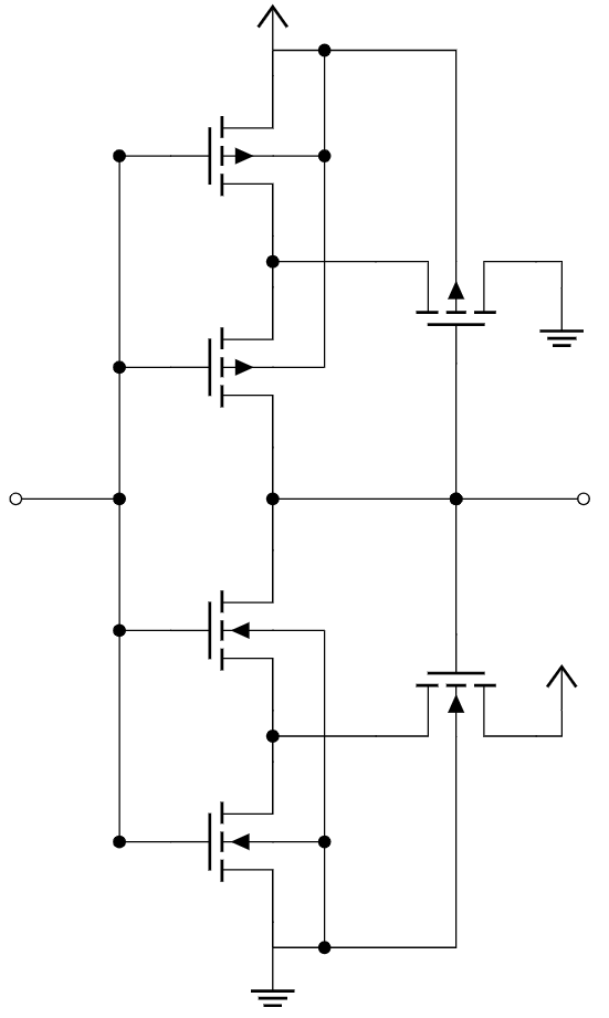
SNSPDs#

A biasing current, denoted as \(i_{d}\), typically in the microampere (\(\mu A\)) range, needs to be applied across the SNSPD detector in its superconducting state.
WWhen the SNSPD is superconducting, \(R_{SNSPD} = 0\), meaning no photons are detected. According to Ohm’s law \(V=iR_{SNSPD}\), there is a short circuit across the SNSPD. The currents in each node of the interconnected SNSPD circuit model in Figure [1] are derived from Kirchhoff’s current law in Equation [2]. The total biasing current applied to the detection component subsystem, \(i_b\), is divided across the parallel terminator resistor current \(i_{TERM}\) and the SNSPD detector biasing current \(i_b\).
When a photon with energy \(E_p(T) = \frac{\hbar c}{\lambda}\) is absorbed, it creates a resistive hotspot in the SNSPD, making \(R_{SNSPD} \approx k \Omega\). A high-speed voltage pulse is generated from the energy stored in the SNSPD-meander inductor \(E_{L_k}\), as described in Equation [3], flowing across the increasing thermal hotspot due to inductive current \(i_{L_k}\) resistive dissipation. For a fast cooldown of the SNSPD back to the superconducting state, minimizing the inductive current dissipation is essential [1], and no further SNSPD biasing current \(i_d\) is required in its resistive state.
The lowest impedance path for the system-biasing current \(i_b\) in the circuit in Figure [1] is through the parallel terminator resistor \(R_{TERM} \approx 50 \Omega\), designed to match the impedance of the high-speed tapered coplanar waveguide \(R_{TAPER,CPW}\). While the SNSPD is in its non-superconducting state and needs to cool down to reset, the rest of the system biasing current \(i_b\) flows through the terminator resistor to prevent electro-thermal dissipation latching.
The output voltage pulse \(V_{pulse}\) rise time \(\tau_{rise}\) in Equation [4] is related to the shunt combined complex impedance of the coplanar waveguide and the terminator \(Z_{load}\), with the RF interconnection standard 50 \(\Omega\) impedance. The reset time of the detector is also related to the shunt load impedance and the inductive energy dissipation in Equation [5] [2, 1].
The energy dissipated at the SNSPD hotspot immediately during photon absorption \(E_p(T) = \frac{\hbar c}{\lambda}\) can be expressed in relation to the superconducting-biasing current \(i_s\).
References
Annunziata, A. J., Santavicca, D. F., Frunzio, L., Catelani, G., Rooks, M. J., Frye, D., … & Prober, D. E. (2010). Reset dynamics and latching in niobium superconducting nanowire single-photon detectors. Journal of Applied Physics, 108(8), 084507.
Kerman, A. J., Dauler, E. A., Keicher, W. E., Yang, J. K. W., Rosfjord, K. M., & Berggren, K. K. (2006). Kinetic-inductance-limited reset time of superconducting nanowire photon counters. Applied Physics Letters, 88(11), 111116.
Transmission Lines#
TODO properly write this section.
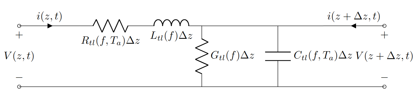
Properties#
Taken from [1] Eq 2.49
Terminated Lossless Transmission Line Fig 2.4 Interface to terminating load at \(z=L\)
\(Z_L \ne Z_0\) for incident wave form \(V_0^+ e^{-j\beta z}\) at \(z<0\). Ratio voltage to current is \(Z_0\)
Current on the line .. math:
i(z) = \frac{V_0^+}{Z_0} e^{-j\beta z} - \frac{V_0^-}{Z_0} e^{j\beta z}
Standing waves in line
Time averaged power flow along the line at a given \(z\) for a set \(f\) frequency
Note that \(\Gamma^* e^{-2j\beta z} + \Gamma e^{2j\beta z}\) TODO give an imaginary result in the form \(A - A^* = 2j Im\{ A\}\) which is imaginary. (Note this is only for a lossless transmission line)
In this case:
When mismatched
where \(l=-z\)
First Principles#
The conductive current is the dominant current effect over displacement current if the conductivity \(\sigma >> w \epsilon\) dielectric-frequency condition is satisfied on a “good conductor” material [1].
Phase index according to [2]
Transmission Line Telegrapher’s Equations#
[3]
Based on [2]
Conductive loss:
The complex permittivity of the medium \(\epsilon(f,T_a)\)
Dielectric loss related to imaginary part of complex permittivity \(\epsilon^{''}(f,T_a)\)
\(G_0\) DC dielectric loss.
Total dielectric loss:
Parallel plate parasitic capacitances between in \(SiO_2\)
TODO validate frequency, temperature source. \(\epsilon_{SiO_2}(f = DC,T_a = 300K) = 3.9\)
Distributed junction capacitance and resistivity of the small signal equivalent circuit of the junction is bias, temperature and voltage dependent. Per Patel Effective relative permittivity approximated as average capacitances in substrate and superstrate ignoring dispersion and cross section of transmission line, conductor shape. Higher frequencies permittivity smaller than 3.4
References#
Pozar, David M. Microwave Engineering. John Wiley & Sons, 2011.
Patel, K. Design and Analysis of Microwave Circuits. Academic Press, 2015.
Wadell, Brian C. Transmission Line Design Handbook. Artech House,